Nintendo Switch Oled Schematics
Nintendo switch oled review Nintendo switch, repairing damaged or lifted pads on usb-c port! Motherboard gbatemp values losing mostly
Switch OLED teardown V1/V2 | Page 42 | GBAtemp.net - The Independent
Nintendo switch oled : lancement officiel le 8 octobre et on connaît Nintendo switch circuit diagram Ask the developer, nintendo switch – oled model
Nintendo switch schematic diagram
[info] board diagram and part numbersNintendo switch oled mod chip Oled hwfly success! be careful with that lcd connector, how i replacedUnpatched v1 nintendo switch.
Info] board diagram and part numbers nintendo switch, 40% offJoycon charges detecting 2373 1514 pinouts gbatemp tronicsfixforum side2 Nintendo switch oled model user manualNintendo switch schematic // sd card parts.

Oled nintendo switch teardown
[ベスト] nintendo switch usb pinout 104639-nintendo switch usb pinoutSwitch oled teardown v1/v2 Oled nintendo switch teardownIfixit takes a nintendo switch oled for a teardown – malibbuinc.
Nintendo switch schematic // sd card partsGame knights 上 nintendo switch pcb board 136541-nintendo switch pcb boardNintendo tronicsfixforum.

Nintendo switch lite schematic diagram pdf
[info] board diagram and part numbersTechinsights teardown: nintendo switch oled handheld game console Geçici ad armstrong sapihten kaçış nintendo switch motherboard diagramNintendo switch oled model set up manual guide.
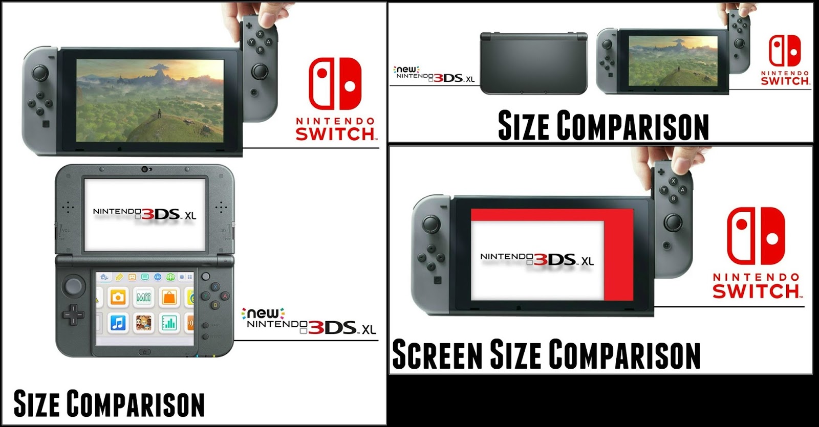
Nintendo switch board draws 0.46 a and doesnt bootOled announces ekran anuncio zapowiedziano premiery jest xfire Switch oled teardown v1/v2Switch nintendo size 3ds console xl screen comparisons appears cons joy body main so.

Nintendo switch – oled model console diagram
[help] switch oled modchip alternative point上 nintendo switch pcb board 136541-nintendo switch pcb board For nintendo switch console motherboard pcb board repair charging portNintendo switch schematic diagram.
M0 trinket switch nintendo modchip board gbatemp guide internal gemma itsybitsy samd21 express support laid solderNintendo has announced the ‘nintendo switch oled model’ Nintendo switch lite circuit board diagram.


![[INFO] Board diagram and part numbers - Nintendo Switch - TronicsFix](https://i2.wp.com/www.tronicsfixforum.com/uploads/db3735/original/1X/50b0c129da91f3a1611ec1151664658204217c3a.jpeg)


